
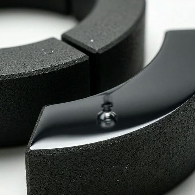
Visual Acceptance Standards for Ferrite Magnets: Managing Edge Chipping and Cracks
Define visual defect limits for custom ferrite magnets: classify edge chips and cracks, set AQLs, and align supplier inspection before RFQ or PO release.
When sourcing custom ferrite magnets for mass production, one of the most common and costly sources of friction between OEMs and magnet suppliers is the subjective evaluation of visual defects. Unlike machined metals or plastic injection-molded parts, ferrite magnets are sintered ceramic materials. Their inherent brittleness, combined with the mechanical stresses of grinding, tumbling, and magnetization, guarantees that minor edge chipping and micro-cracking will occur. For procurement teams and quality engineers, the challenge is not eliminating chips entirely—doing so would drive costs to uncompetitive levels—but rather defining clear, objective visual acceptance standards that distinguish between cosmetic imperfections and functional defects.
This playbook provides a deep dive into establishing robust visual acceptance criteria for hard ferrite magnets. It is designed to help OEM buyers, SQA (Supplier Quality Assurance) managers, and mechanical engineers align on defect definitions, establish practical Acceptable Quality Limits (AQL), and integrate these standards into their RFQ and PO processes to ensure stable, cost-effective supply chains. By moving away from subjective "looks damaged" assessments to quantifiable metric-driven acceptances, companies can significantly reduce their scrap rate and optimize material cost.
Applicability Boundaries and Scope of Standards
Before diving into the quantitative defect metrics, it is vital to establish the applicability boundaries of these visual standards. Ceramic ferrite magnets are utilized across a vast spectrum of applications, from low-cost promotional items to highly engineered automotive sensors and brushless DC (BLDC) motor rotors. The acceptance criteria must scale with the application's functional criticality.
The standards outlined in this guide are primarily applicable to industrial, automotive, and consumer electronics applications where the magnet serves a functional purpose (e.g., motors, actuators, sensors, acoustic drivers). They are not intended for consumer-facing aesthetic applications (like refrigerator magnets) where the surface finish is the primary selling point.
Furthermore, these guidelines apply specifically to sintered hard ferrite (ceramic) magnets. They should not be extrapolated to Neodymium Iron Boron (NdFeB) or Samarium Cobalt (SmCo) magnets. NdFeB magnets, for instance, are highly prone to corrosion and are usually plated; a chip in a Neodymium magnet compromises the protective coating and can lead to rapid oxidation and catastrophic failure. Ferrite magnets are oxide ceramics and do not rust, making cosmetic edge chips far less hazardous to the long-term operational lifespan of the part.
The True Cost of Undefined Visual Standards
In the absence of a mutually agreed-upon visual standard, incoming inspection teams typically default to "zero tolerance" for chips and cracks. When dealing with ceramic ferrites, this approach can push rejection rates into double-digit territory even on lots that are entirely functionally sound. The downstream consequences of ambiguous visual criteria include several severe financial and operational penalties:
- Inflated Piece Price: Suppliers are acutely aware of their customers' rejection habits. If a supplier knows your incoming inspection is aggressively rejecting cosmetic chips, they will factor a massive scrap allowance into your piece price during the RFQ phase. You end up paying a premium for perfectly good magnets that were preemptively thrown away.
- Supply Chain Disruptions: Unexpected lot rejections at your receiving dock lead to immediate material shortages, potential line down situations, and the necessity of expedited freight costs to rush replacement parts from overseas.
- Friction in Supplier Relationships: Continuous disputes over "how big is too big" for a chip degrade trust and partnership. Top-tier suppliers may prioritize customers with more rational, data-driven quality requirements, leaving you with less capable vendors.
- Delayed Time-to-Market: Engineering and quality assurance time is wasted reviewing deviation requests and MRB (Material Review Board) dispositions for cosmetic issues instead of focusing on core product development and continuous improvement.
To avoid these hidden costs, OEMs must transition from subjective visual checks to objective, measurable criteria, fully documented within the mechanical drawing and quality agreement.
Use this visual standard with the Ferrite RFQ checklist, the ferrite magnet tolerance guide, and the packaging and logistics guide so drawing notes, inspection plans, and transit controls use the same defect language.
Visualizing Edge Chipping: Working vs. Non-Working Surfaces
To better understand how defects are classified, it is helpful to visualize the anatomy of a typical magnet and where defects commonly occur. The following SVG diagram illustrates the critical difference between a chip on a working surface versus a non-working surface.
The foundational step in creating a visual standard is recognizing that not all surfaces on a magnet are equally important. A 2mm chip on the pole face might disrupt the magnetic flux profile, while the same 2mm chip on a non-magnetic mounting edge is entirely irrelevant.
Working Surfaces (Functional Areas)
Working surfaces are the faces of the magnet that actively contribute to the magnetic circuit. These include:
- The primary magnetic pole faces (e.g., the flat faces of an axially magnetized disc).
- Surfaces that mate tightly with a yoke, back iron, or pole piece where an air gap would cause significant permeance loss.
- Areas where a Hall effect sensor directly reads the magnetic field.
Defects on working surfaces directly impact the functional output of the magnet. Therefore, the visual acceptance criteria for these areas must be significantly tighter. Chipping here reduces the effective volume of the magnetic material, slightly lowering total flux, and can cause localized field distortions which could induce jitter in encoder applications.
Non-Working Surfaces (Cosmetic/Structural Areas)
Non-working surfaces are the edges or faces that do not primarily direct magnetic flux and are not critical to the magnetic circuit. These include:
- The outer diameter (OD) of a cylinder that only serves to hold the magnet in a plastic housing (provided the chip doesn't compromise adhesive bonding).
- Chamfered edges designed specifically to relieve stress and prevent sharp-corner chipping.
- Surfaces that will be completely encapsulated in overmolded plastic or potted in resin.
For non-working surfaces, the visual standards should be relaxed considerably. The primary concern here is not magnetic performance, but rather mechanical integrity (ensuring the chip isn't actually a propagating crack) and cleanliness (ensuring no loose ferrite powder contaminates the assembly).
Structural Defects: Cracks, Chips, and Burrs
To quantify defects and accurately communicate with suppliers, we must clearly define the terminology used during inspection. Furthermore, it is critical to understand the specific failure risks associated with each defect type.
Edge Chipping (Spalling)
Chipping occurs when small pieces of the ceramic material break away from the edges or corners during grinding, handling, or transit. Because ferrites are brittle, sharp 90-degree corners are highly susceptible to chipping. Failure Risk: Loose magnetic particles can detach during operation, migrating into bearings or electrical contacts, causing premature mechanical failure. Engineering Tip: Always design custom ferrite magnets with chamfered or radiused edges (e.g., a 0.5mm x 45° chamfer) to drastically reduce chipping during bulk handling.
Cracks (Hairline and Structural)
Cracks are fissures within the material, presenting the highest risk of catastrophic failure.
- Hairline Cracks (Surface Crazing): Often caused by thermal shock during the sintering or cooling process. If they do not penetrate deeply and do not compromise structural integrity, they are sometimes acceptable depending on length.
- Structural Cracks: Deep fissures that threaten to split the magnet under mechanical stress or thermal cycling. Failure Risk: If a structurally cracked ferrite magnet is installed in a high-speed motor rotor (e.g., a BLDC power tool motor spinning at 20,000 RPM), centrifugal forces can cause the magnet to explode inside the stator, completely destroying the application. These are always critical defects.
Pull-outs (Pitting)
Pull-outs are small voids on the surface where a grain or cluster of grains was torn away during the grinding process. These look like small craters and are generally acceptable up to a certain diameter, as they rarely affect magnetic output. Failure Risk: Virtually zero, provided the pitting is not so extensive that it reduces the overall mass of the magnet below specification.
Specification Dimensions and Measurement Methodology
Defining the limits is only half the battle; establishing how those limits are measured and dimensioned in CAD is equally critical to prevent disputes.
1. Naked Eye Inspection Standard
Visual inspection should be conducted without magnification (no microscopes or loupes) at a distance of 30 cm (approx. 12 inches) under standard fluorescent or LED lighting (typically 500 to 1000 lux). The inspector should view the part for no more than 3 to 5 seconds. If a defect cannot be seen under these conditions, it should not be considered a defect. Using 10x magnification to find micro-chips on a standard industrial ferrite magnet is a misapplication of quality control resources and will lead to false rejections.
2. Defect Measurement and CAD Dimensioning
When a defect is identified visually, it should be measured using calibrated digital calipers, an optical comparator, or a vision system if precise boundary validation is required. For edge chips, measure the maximum linear dimension along the edge (Length) and the maximum depth penetrating into the face (Depth). In your engineering drawings, use Geometric Dimensioning and Tolerancing (GD&T) to specify surface profile tolerances in critical zones, explicitly referencing international standards like IEC 60404-8-1 where applicable.
3. The "Fingernail Test" for Cracks
To differentiate between a harmless surface scratch (or tooling mark) and a hairline crack, inspectors often use a simple tactile test. If a fingernail catches on the line, it is a physical fissure (crack). If it glides smoothly, it is likely a surface mark or superficial crazing.
4. Loose Particle Testing (Cleanliness)
Because chipped ferrites can shed magnetic dust, a critical inspection step for sensitive applications is the tape test. Apply a standard adhesive tape to the surface and peel it off. A light residue of ferrite dust is normal, but chunks or large flakes indicate severe micro-fracturing that will cause contamination downstream.
Quantitative Visual Acceptance Table (Baseline Standard)
The following table provides a recommended baseline for visual acceptance of custom ferrite magnets in standard motor, sensor, and acoustic applications. These limits should be adjusted based on the specific size of your magnet. Note: Dimensions below assume a typical medium-sized ferrite magnet (e.g., 20mm to 50mm OD). These are RFQ starting limits, not universal ISO, IEC, or MMPA cosmetic requirements; validate them against functional flux testing, dimensional inspection, and supplier process capability before release.
| Defect Type | Surface Classification | Maximum Acceptable Limit (Individual Defect) | Cumulative Limit per Part | Rejection Criteria (Critical) |
|---|---|---|---|---|
| Edge Chipping | Working Surface | Length ≤ 1.5mm, Depth ≤ 0.5mm | Max 2 chips per face | Any chip altering the pole profile geometry |
| Edge Chipping | Non-Working Surface | Length ≤ 3.0mm, Depth ≤ 1.0mm | Max 3 chips per edge | Chip compromises adhesive bonding area |
| Corner Chipping | All Corners | Missing volume ≤ 2.0mm³ | Max 2 corners affected | Sharp, un-tumbled jagged edges remaining |
| Surface Pitting | Working Surface | Diameter ≤ 1.0mm, Depth ≤ 0.5mm | Max 3 pits per face | Clustered pitting covering >5% of area |
| Surface Pitting | Non-Working Surface | Diameter ≤ 2.0mm, Depth ≤ 1.0mm | No strict limit if scattered | Pits penetrating >10% of magnet thickness |
| Cracks | Any Surface | Hairline (non-penetrating) ≤ 5.0mm length | Max 1 crack per part | Any structural, penetrating crack |
| Tooling Marks | Any Surface | Acceptable if depth ≤ 0.2mm | N/A | Scratches creating stress risers |
Procurement & Engineering Decision Matrix: Quality vs. Cost
When establishing acceptable quality limits (AQL) for custom ferrite magnets, cross-functional teams must balance functional requirements against piece-price impact. The following decision matrix outlines key considerations and buyer decision points across six typical application scenarios, ensuring procurement and engineering are aligned. The cost impacts below are directional RFQ planning estimates; confirm actual deltas with supplier quotations because magnet size, chamfer design, packing method, and inspection automation can change the economics.
| Application Scenario | Functional Criticality | Typical Tolerance for Chipping | Recommended AQL | Cost Impact of Strict Visuals | Buyer Decision Point | Supplier Communication Focus |
|---|---|---|---|---|---|---|
| High-RPM BLDC Rotors | Critical (Balance & Flux) | Very Low | 0.40 - 0.65 | Very High (+40%) | Validate if 100% automated vision inspection is justified vs manual sorting. | Require SPC data on chamfer dimensions and zero-crack policy. |
| Precision Hall Sensors | Critical (Localized Flux) | Low | 1.0 | High (+25%) | Balance localized chip limits directly over the exact sensor read area. | Specify exact working surface mapping in 2D drawings. |
| Standard DC Brush Motors | Moderate | Medium | 1.5 - 2.5 | Moderate (+10%) | Accept minor edge chips that do not cross the arc radius or affect bonding. | Emphasize layer packing to prevent transit damage. |
| Acoustic / Speaker Rings | Low (Total Flux Volume) | High | 4.0 | Low (Baseline) | Focus on total magnetic mass rather than cosmetic edges. | Set loose visual criteria; prioritize dimensional stack-up. |
| Magnetic Separators | Very Low | Very High | 6.5 | Negative (Cost Save) | Accept unchamfered blocks with significant cosmetic damage for raw material savings. | Request lowest-cost bulk packaging if damage doesn't matter. |
| Overmolded Assemblies | Low (Mechanical only) | Medium | 2.5 - 4.0 | Low (Baseline) | Ensure chips do not create loose powder that fouls injection molds. | Specify tape-test cleanliness and no structural cracks. |
Visual Standards Checklist for OEM Procurement
To ensure flawless execution and avoid mid-production disputes, procurement teams must integrate visual standards into the sourcing lifecycle. Use this checklist when qualifying a new ferrite supplier, sending out RFQs, or launching a new custom magnet.
- Define Surfaces on Drawings: The 2D engineering drawing explicitly calls out Working vs. Non-Working surfaces.
- Specify Edge Treatments: Edges are specified with chamfers (e.g., C0.5) or radiuses (e.g., R0.5) to prevent sharp-edge chipping.
- Include Quantitative Table: A visual defect matrix (similar to the table above) is embedded directly in the drawing notes or attached as a formal Quality Specification.
- Define Inspection Method: The PO or Quality Agreement specifies "Naked eye, 30cm distance, 5 seconds" to prevent over-inspection.
- Establish Boundary Samples: During the PPAP (Production Part Approval Process) or First Article Inspection, request the supplier to provide physical "Limit Samples" (one showing an acceptable chip, one showing a rejectable chip) and sign off on both.
- Align AQL Levels: Agree on the Acceptable Quality Limit (e.g., AQL 1.0 for major functional defects, AQL 2.5 for minor visual defects) based on ISO 2859-1 sampling plans.
- Document Supplier Communication Fields: Ensure the supplier RFQ template includes specific fields acknowledging the AQL, packaging method, and boundary sample requirements.
FAQ: Navigating Ferrite Visual Quality
Q1: Why do ferrite magnets chip so much more easily than neodymium magnets? Ferrite (ceramic) magnets are manufactured through a pressing and sintering process, resulting in a crystalline ceramic structure. Unlike neodymium magnets, which contain metallic elements and are usually protected by a robust metallic plating (like Ni-Cu-Ni or Zinc), ferrites are unplated ceramics. They possess high hardness but very low tensile strength and fracture toughness. They behave more like a dinner plate than a piece of steel.
Q2: Will a 2mm chip affect the magnetic strength of my magnet? In most cases, no. The loss of magnetic flux is directly proportional to the loss of magnetic volume. A 2mm chip on a 20mm block represents a fraction of a percent of the total volume. Unless the chip is directly over a highly sensitive Hall sensor reading point, the overall field impact is negligible and will not push the part below the minimum Gauss/Tesla requirement.
Q3: We found hairline cracks in our shipment. Are they safe to use? It heavily depends on the crack's depth and location, as well as the application environment. Surface crazing from thermal stress during manufacturing is common and usually stable. However, deep penetrating cracks can propagate during assembly (especially if press-fit or subjected to thermal cycling in a motor). Structural cracks should always be rejected immediately.
Q4: Should we require a coating on ferrite magnets to prevent chipping? Coating ferrite magnets (e.g., with epoxy) is generally not recommended for cost reasons. The cost of coating often negates the primary advantage of choosing ferrite (low cost). Instead, invest in better part design (larger chamfers) and better visual acceptance alignment.
Q5: The supplier shipped magnets bulk-packed in bags, and they are heavily chipped. Who is at fault? If bulk packaging was specified to save costs, the buyer must accept a higher degree of chipping. Ferrite magnets attract each other violently. Bulk packing allows them to crash together during transit, causing severe edge chipping. To prevent this, OEMs must specify layer-packing (using cardboard or foam separators) in the RFQ.
Q6: How do international standards like MMPA 0100-00 handle visual defects? Standards like MMPA 0100-00 provide overarching guidelines on material properties and testing, but they leave specific visual cosmetic acceptance criteria up to the mutual agreement between the buyer and the manufacturer. This is exactly why custom boundary limit samples and explicit drawings are required; standard industry documents do not provide universal size limits for chips.
Best Practices for Packaging to Prevent Secondary Chipping
Even if a supplier produces perfect magnets and inspects them flawlessly, improper packaging will ruin them before they arrive at your dock. Because magnetized ferrites attract each other with significant force, allowing them to snap together across air gaps will instantly shatter edges.
- Avoid Bulk Packing: Never allow custom ferrite magnets to be shipped loose in bags or boxes, except for very small, non-critical isotropic craft magnets.
- Layer Packing: Require magnets to be packed in organized layers, separated by thick cardboard or EPS foam sheets.
- Orient for Neutralization: Magnets should be arranged in alternating polarity configurations within the box to neutralize the external magnetic field and reduce the force with which they pull towards each other.
- Vacuum Sealing: For highly critical parts, vacuum sealing layers in plastic prevents any relative movement during vibration in transit.
- Drop Test Validation: For large shipments, require the supplier to perform ISTA drop tests on the master carton to ensure the internal separators do not collapse under the immense weight of the dense ferrite material.
References and Source Notes
- ISO 2859-1:2026 Sampling procedures for inspection by attributes supports the article's AQL sampling-plan references.
- IEC 60404-8-1:2015 Magnetic materials - specifications for magnetically hard materials supports the magnetic-material specification context.
- MMPA 0100-00 Standard Specifications for Permanent Magnet Materials supports permanent magnet material property and terminology context.
These references do not publish one universal chip-size acceptance table for every ferrite geometry. The quantitative limits in this article are buyer-supplier agreement baselines intended to be validated with boundary samples, functional magnetic testing, and application risk review.
Conclusion: Align Visual Standards Before PO
Ambiguous visual standards lead to unnecessary rejections and inflated costs. By clearly defining working vs. non-working surfaces and setting quantifiable limits on chipping, OEMs can stabilize their ferrite magnet supply chain and reduce friction.
Recommended Action
Incorporate a quantitative visual acceptance matrix into your engineering drawings and mandate physical boundary limit samples during the First Article Inspection phase.
Caution
Do not apply NdFeB (Neodymium) visual standards to ceramic ferrite; their mechanical properties, manufacturing processes, and failure modes are fundamentally different.
How FerriteCustom Supports Your Quality Goals
At FerriteCustom, we understand that quality is defined by consistency and clarity. We work directly with OEM engineering and procurement teams during the RFQ phase to review 2D drawings, recommend edge chamfers for manufacturability, and agree on practical, cost-effective visual acceptance standards.
By defining limits upfront and providing signed boundary samples with PPAP documentation, we ensure that the magnets you receive match your functional needs without unnecessary scrap costs.
For a review of your custom ferrite magnet drawing or to discuss AQL limits for your next project, contact our quality engineering team at [email protected].
Evidence and Applicability Notes
Last reviewed: 2026-07-23
Sources Used
- [ISO 2859-1:2026 Sampling procedures for inspection by attributes](https://www.iso.org/standard/85464.html)
- [IEC 60404-8-1 Magnetic materials - Specifications for individual materials](https://webstore.iec.ch/en/publication/22009)
- [MMPA 0100-00 Standard Specifications for Permanent Magnet Materials](https://allianceorg.com/pdfs/MMPA_0100-00.pdf)
Method
- Mapped common OEM SQA inspection decisions for motor, sensor, acoustic, separator, and overmolded ferrite applications
- Compared brittle ceramic failure modes with magnetic-circuit sensitivity by working and non-working surface
- Used ISO 2859-1 sampling logic, IEC magnet material specification context, and MMPA material property terminology as reference boundaries
Applicability Boundary
- Standards provided are baseline recommendations; highly sensitive applications (e.g., aerospace, high-precision encoders) may require tighter, customized limits.
- Visual standards do not replace functional magnetic flux testing or dimension verification.
Author

Categories
More Posts
CEN/TS 18263:2026 Permanent Magnet Labeling: A Sourcing Guide for Ferrite Buyers
Learn how CEN/TS 18263:2026 affects custom ferrite magnet RFQs, supplier audits, labeling data, and EU DPP readiness before 2026 sourcing programs launch.

Ferrite Market Update (2026-W20): HTS Revision 7, US Comment Window, and EU Raw Materials Mechanism Controls
Decision brief for ferrite magnet buyers on April-May 2026 trade-classification and raw-material sourcing signals that can change RFQ, landed-cost, and release controls.

Ferrite Cost Advantage and Average Price Calculator
Estimate the average ferrite magnet price and convert quote-line pricing into a landed cost model with tooling, yield, logistics, and risk reserves.
Inquiry Email
Copy the email, or open your default email app to start an inquiry.